Continued from Part 2 -- Circuit Description.
|
|
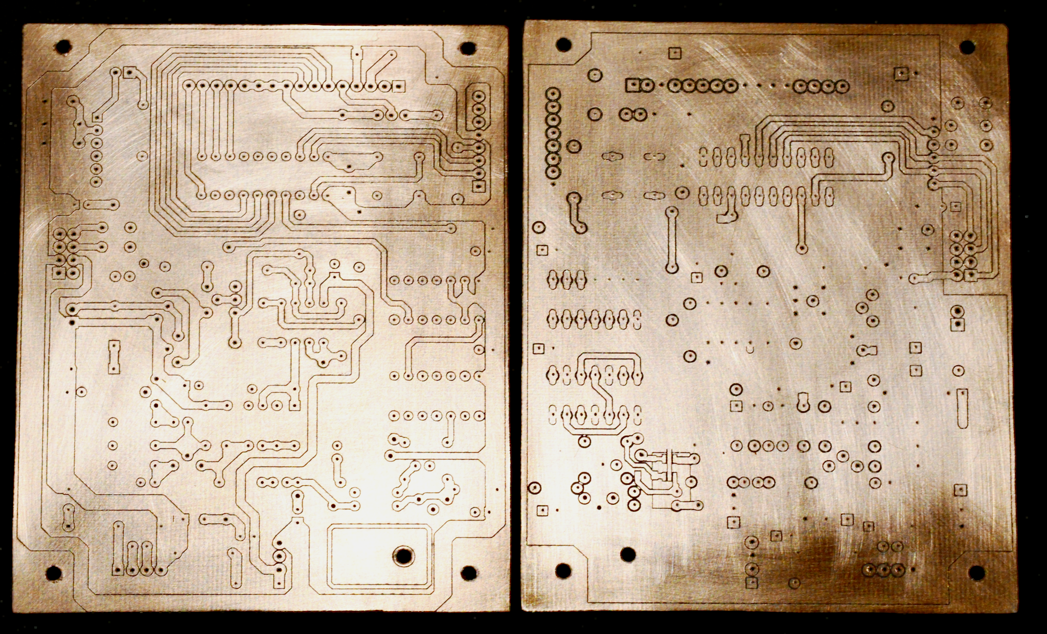
| Figure 4: Printed-circuit board from the PCB mill, solder side (left) and component side (right). Most of the component side copper serves as ground plane. Click on the image to access a full-size version. |
Ground-plane design: Most of the component side copper was realized as ground plane. Ground plane layout designs provide for more rugged and reliable RF circuits (see, for example, Linear Technology's AN-47). Some of the area is excluded from the ground plane, because external connectors and standoffs should not by default be connected to ground. A small SMT region is also excluded, because the thin grooves between traces are easily shorted, and a short (for example, by a flake of copper or solder) is difficult to find.
Incorrect interpretation of the Gerber files: The PCB mill interpreted some of the larger polygonal regions incorrectly. For example, the trace that connects TP1, the base of Q1 and the collector of Q2, was not cut out of the ground plane. Some less significant mistakes that the PCB mill software made included notably some of the IC ground and supply connections. These mistakes were remedied with an x-acto knife. The PCB layout had only one real design mistake -- the AGC level input to of the microcontroller was connected to the wrong op-amp output; this mistake is corrected in the PCB and Gerber files that can be downloaded from this page.
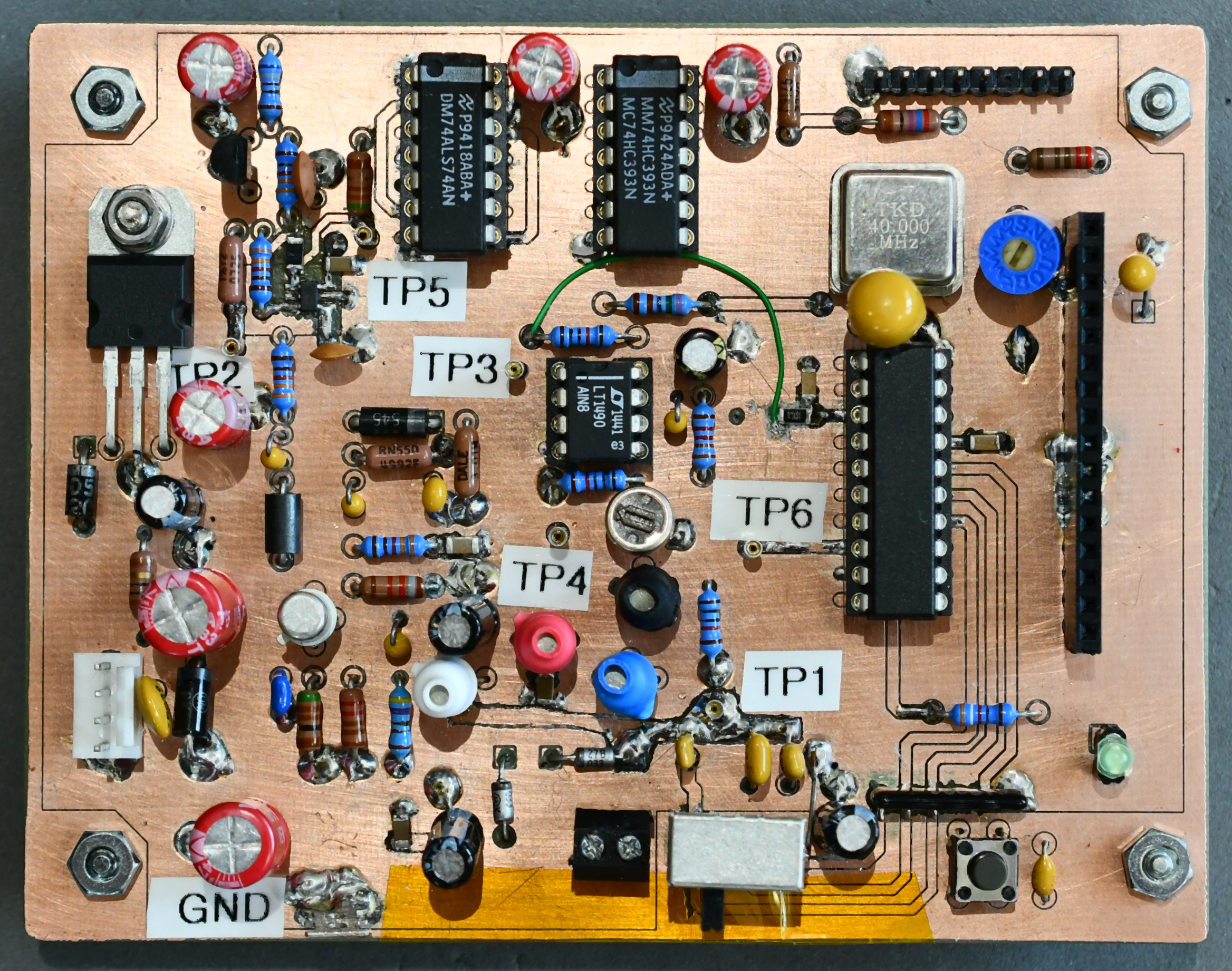
The complete assembled board is shown in Figure 5. The layout mistakes above are visible: Near TP1, a hand-routed trace is visible. A green jumper wire carries the correct amplitude signal to the microcontroller. Note the small SOT-89 comparator left of TP5. Also note that for easier identification the oscillator transistors were color-coded with colored shrink tube (1 - red; Q2 - blue; Q3 - black; Q4 - white; no shrink tube for Q5).
|
| Figure 5: Completely populated and soldered PCB. The transistors were fitted with colored shrink tube sleeves to distinguish them more easily (Q1 - red; Q2 - blue; Q3 - black; Q4 - white). One component-side trace that the PCB mill's software did not interpret correctly was manually scratched out (near TP1), and one layout mistake had to be corrected (green wire to pin 3 of the MCU). Testpoints were realized with individual pins from machine-tooled IC sockets. Click on the image to access a full-size version. |
|
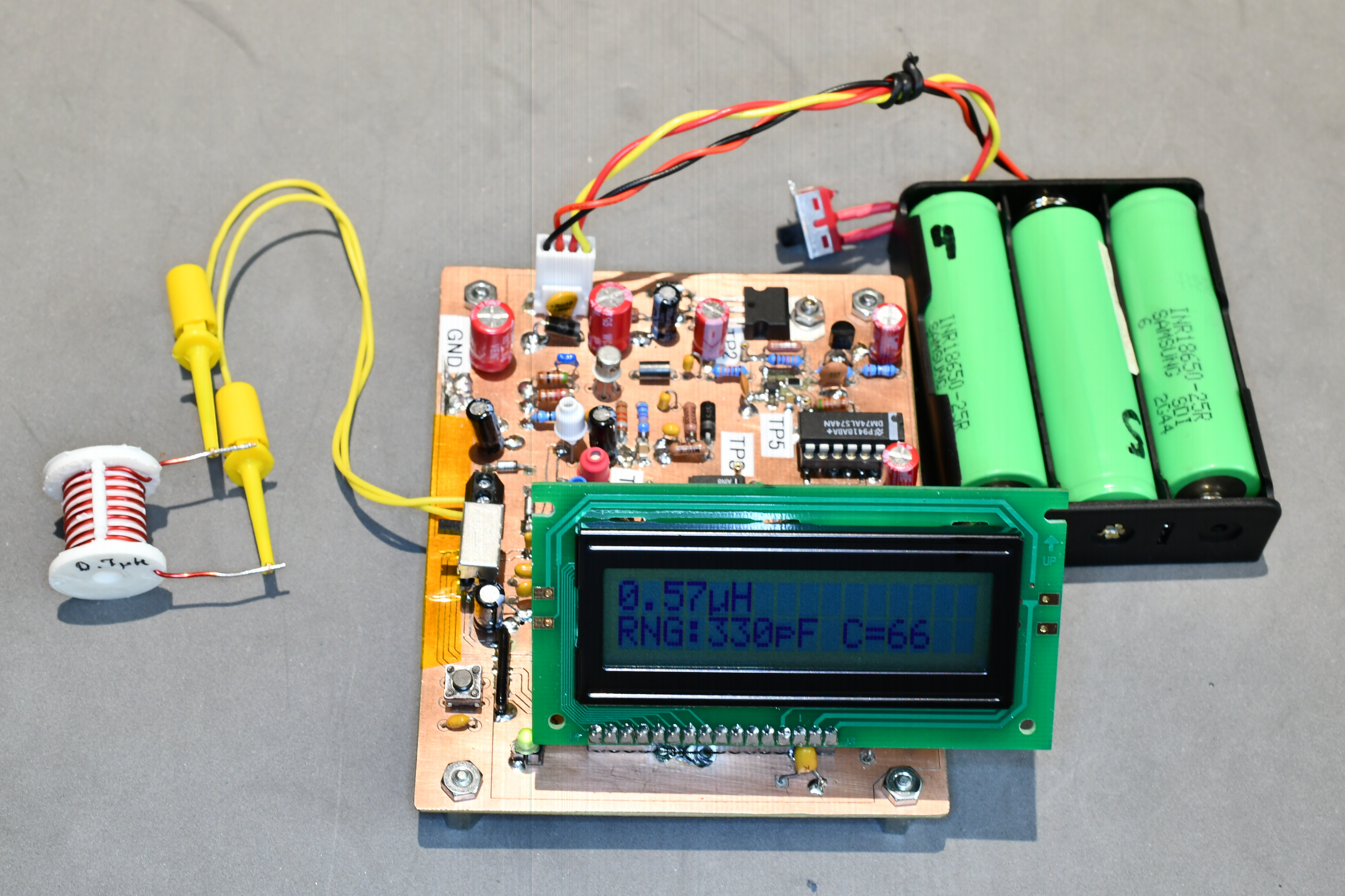
| Figure 6: Soldered PCB (Figure 5), assembled in the the complete device. The LCD is plugged directly into the header on the PCB, its pins bent 45° backward. Battery pack and switch can be recognized. A sample coil is connected to the pins. The inductor formula suggests 0.7μH, and the device indicates 0.56μH. This is not a bad match when tolerances of the coil former are considered. Click on the thumbnail for a full-size image. |
|
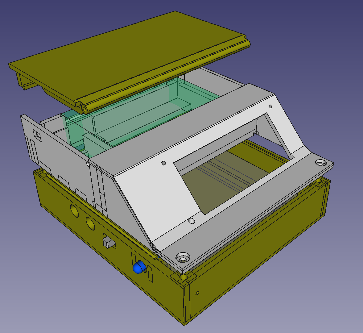
| Figure 7: FreeCAD design of an enclosure for the electronics. Click on the thumbnail for a full-size image. |
|
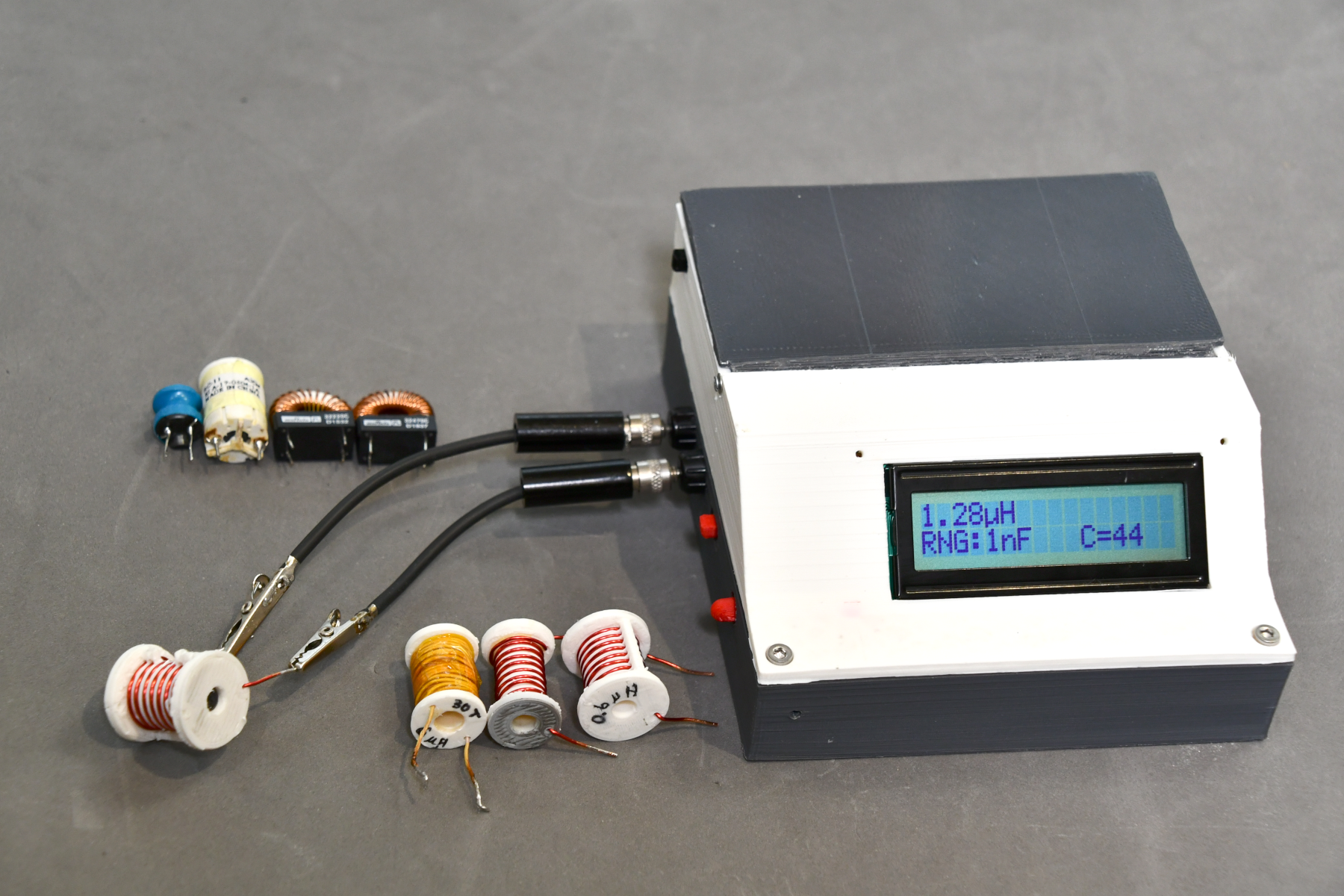
| Figure 8: View of the complete device in its enclosure. The batteries are accessible underneath the gray cover, which swings upward on hinges. on the left side, there is the power switch (far back) and the red capacitor selector and display function pushbutton. A selection of home-made and commercial inductors can be seen. |
The comparison failed, however, when inductors of less than 10μH were used, because the commercial RLC meter's accuracy was degraded. For fixed inductors with an inductance label, tolerances were not exceeded. Unfortunately, there was no reference standard available for small inductors.
The situation was remedied as follows. Equation 1 in Part 1 indicates a relationship of \( L \propto N^2 \) where \( N \) is the number of turns. This proportional relationship is rooted in the physics of self-induction and is not an approximation. A coil with a comparatively large number of turns can be measured with both devices. By iteratively removing one turn and re-measuring the coil, the diminishing inductance should be seen.
|
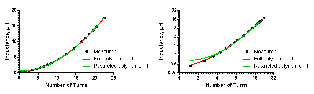
| Figure 9: Precision assessment by iterative removal of one turn of a coil in linear scale (left) and double logarithmic scale (right). The log-log scale reveals an apparent horizontal asymptote at low inductances. Click on the thumbnail for full-size image. |
Results of such an experiment are shown in Figure 9. Nonlinear regression was performed on the data set (black circles), and two alternative models were used. The full polynomial fit,
\[ L = a {N^2} + b N + L_0 \]
is the statistically preferred model over the restricted model with \( b=0 \) and \( L_0 = 0 \),
\[ L = a {N^2} \]
but it is not justified by Physics. The relative discrepancy between measured data and model is largest at the low-inductance end. A double logarithmic plot (Figure 9, right) reveals more clearly that the reported inductance in the low-inductance range becomes asymptotically horizontal. The explanation, which can be supported experimentally, is that the leads and contacts contribute to the inductance by adding a constant offset. The experimental support comes from using varying lengths of lead wires and from twisting the lead wires: The wires seen in Figure 5 contribute approximately 200nH untwisted and less than 50nH twisted.
Moreover, the parasitic capacitances of Q1, Q2, and Q4 as well as the copper-to-copper capacitance of the PCB add several tens of pF to the resonant tank capacitance, which causes a noticeable deviation of the frequency from the resonant frequency that is calculated from the given capacitor values of C1, C2, and C3. The calibration equation was therefore formulated as
\[L = \frac{1}{(2 \pi f)^2 } \cdot \frac{1}{C + C_0} - L_0 \]
where \( f \) is the measured frequency, \( C \) is the capacitor (C1, C2, or C3), \( C_0 \) is the total parasitic capacitance, and \( L_0 \) is the offset inductance of the PCB traces and the test leads.
Calibration: Roughly 25 fixed inductors in the value range from 1μH to 100μH with nominal inductance were collected (some of them are displayed in Figure 8). The inductance was measured with this device and compared to the nominal inductance, whose tolerances were assumed to have a zero mean. The calibration constant \( a = \left( ( 2 \pi)^2 (C + C_0) \right)^{-1} \) and the wire inductance \( L_0 \) were obtained by nonlinear regression. The new constants were programmed into the software to convert frequency to reported inductance.
Oscillator amplitude: It was interesting to observe that different inductors of the same inductance -- specifically those with different ferrite cores -- can have a widely differing oscillator amplitude. For example, a 2.2μH high-current coil from a buck converter had an oscillator amplitude barely above the cutoff threshold. A 2μH choke, conversely, had an amplitude that was regulated down by the AGC. The oscillator amplitude, displayed as the confidence C during the measurement, appears to be useful to judge a coil's RF capability. RF coils generally have a larger amplitude than high-current ferrite toroid coils. However, this aspect was not further systematically examined.
Schematics, software, and CAD files for the enclosure can be obtained through the links below. Software is copyrighted (C) 2023, M.A. Haidekker, and may be used and distributed under the GNU GPL 3.0 or later. All other files covered under the Creative Commons License CC-BY-SA. The PCB, Gerber files, and schematics were updated in December 2024 to fix minor inconsistencies.
| Schematics | L-Meter Schematics PDF |  |
| Software | Assembly source files PIC18f13k50 Hex File |
 |
| PCB | PCB layout file Gerber files |
|
| Enclosure | Enclosure, complete Enclosure, OBJ files |
|
A note about the software used: The three assembly files in 'firmware.zip' can be used to build a MPLAB-X project. The toolchain is gputils. The project can also be compiled by invoking gpasm/gplink manually from the command line. The PCB was created with gEDA Project's PCB software, but the Gerber files can be viewwed with any Gerber viewer. The enclosure was made with FreeCAD. The zip file contains the Alias Mesh (.obj) files of the individual parts. They can be read directly with, for example, slic3r.
Back to Part 1 of this article.