Printed Circuit Boards -- The Third Way
Part 2
M.A. Haidekker, April 2026
Continued from Part 1 -- Motivation and overview.
STEP BY STEP PREPARATION OF THE PRINTER FILE
1. Create the PCB layout
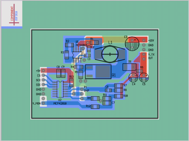
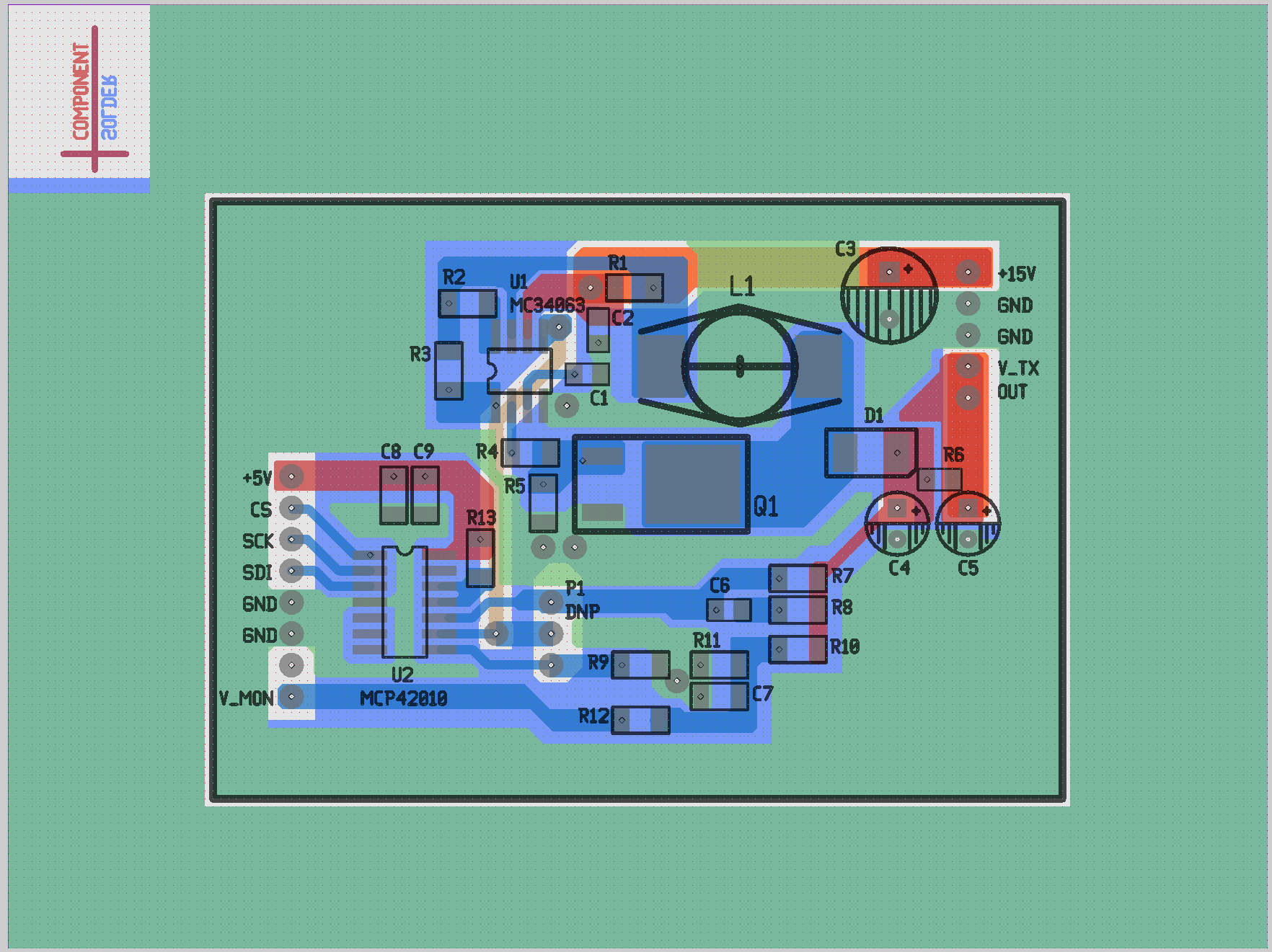
Create the single- or double-sided PCB layout in the usual fashion. Let's use the layout in Figure 1 as an example. The screenshot (from gEDA's PCB software) shows a double-sided layout with most of the solder side used as a ground plane. Even on the same side, different colors were used to highlight trace functions as e.g., power, ground, or signal. Those are later merged on export so that only two sides (solder, component) remain.
|
|
Figure 1: Printed-circuit board layout in gEDA's pcb software. This is a double-sided PCB, but most of the solder side is a ground plane. Note the alignment mark near the top left corner. Click on the image to access a full-size version.
|
When you prepare a PCB for DIY etching, make sure that the solder pads are large enough and that vias and through holes have a very small inner diameter -- the main purpose is to guide the drill, not to instruct a machine what drill size to use. It is also advisable to create custom footprints for SMD components with larger-size landing pads, because those are easier to solder.
2. Export the Gerber files
In the PCB software, choose the option to export Gerber files. This step will generate a series of files of which we only need three:
- Top (component side) copper
- Bottom (solder side) copper
- Plated drill holes (optional: unplated drill holes)
The remaining files, which may contain the solder mask or silk screen, can be ignored.
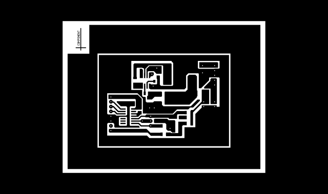
3. Load the Gerber files into gerbv
These instructions refer to gEDA's gerbv; if you use different software, you need to ensure that it has the capability to export image files (PNG, TIFF, etc) at a defined resolution. My Halot-One Plus has a screen resolution of 635 dpi, which means that each pixel must correspond to 1.57/1000 inch (0.04mm) of real PCB space. For example, a PCB of 100mm by 75mm would be represented by 2500 x 1875 pixels. A printer's documentation usually contains the information on the screen resolution.
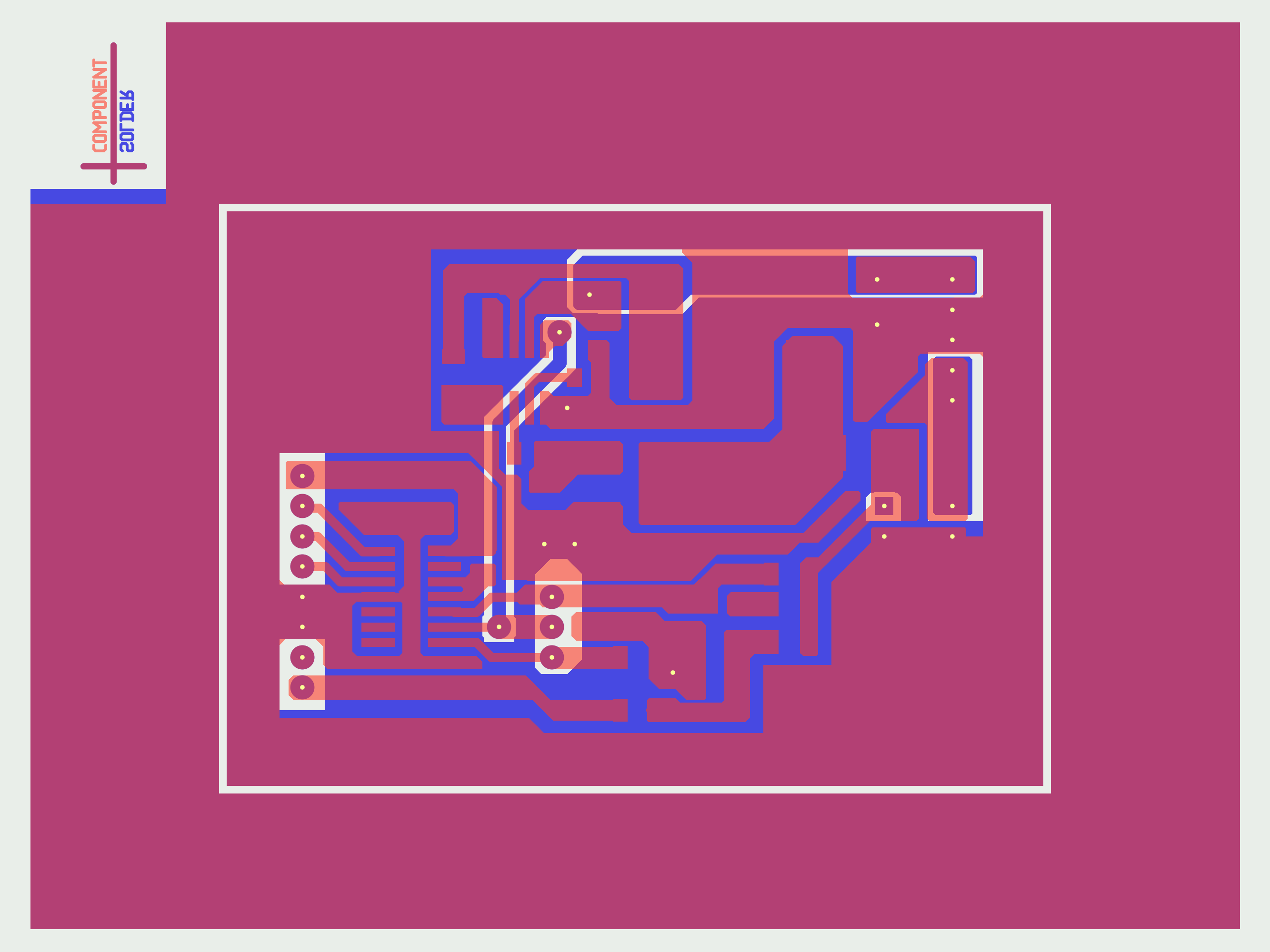
Load the drill file first, set its color to almost-white and transparency to zero. Next, load the solder side copper, color it blue with about 50% transparency. Finally, load the top (component side) copper, give it a red color and also add some transparency. The exact settings are uncritical at this point. The result might look as seen in Figure 2.

|
|
Figure 2: Printed-circuit board from Figure 1 as displayed by the Gerber viewer gerbv. The component side is colored red, the solder side blue, and the drill holes are white. Click on the image to access a full-size version.
|
4. Export the image files for the solder and component sides
We will ultimately need pure black-and-white images with white indicating those regions where the printer exposes the print bed. This means that traces need to be black, and isolation regions white. Drill holes are also white.
- Increase the transparency of the component side so that only a light hint of the component-side traces are visible. This step is optional, and the component side may be temporarily made invisible, but having a shadow of the inactive side makes alignment easier. Decrease the transparency of the solder side so that it is almost opaque. The contrast between solder side traces and isolating regions / drill holes should be strong.
- In gerbv, choose File -> Export -> PNG. Choose a file name (e.g., solder.png) and set resolution to 635 dpi. NOTE: For different printers, different resolutions apply.
- Increase the transparency of the solder side (or make the solder side invisible) similar to what was done with the component side before. Decrease the transparency of the component side.
- In gerbv, choose File -> Export -> PNG. Choose a file name (e.g., component.png) with your printer's resolution (in my case 635 dpi).
Note that, by default, the solder side PNG is mirrored, whereas the component side PNG is not. Also note that single-sided PCBs have only one layer (bottom.png, the solder side).
5. Prepare the image files for conversion into the 3D printer file
For my Halot-One, the file format is cxdlp v.3. For your printer, check out UVTools: you will most likely find a list of resin printers and their associated file formats. Creating the printer file with UVTools is the goal, but we will create a .uvp file as intermediate step.
My 3D printer has a screen size of 4320 x 2560 pixels. I will use these values in this example, and you need to ensure that the image size matches your printer.
- Use the Gimp to create an empty image of 4320 x 2560 pixels, all-black, no transparency.
- Open the previously-created solder.png file in Gimp, copy and paste it into the empty image. The easiest way is to keep the pasted layer centered, but you may arrange multiple PCB layouts onto one PCB, in which case alignment becomes crucial for double-sided PCBs. For single-sided PCBs, alignment is generally not an issue.
- Use the Gimp's layer menu to create a new, fully transparent layer on top of the bottom layer.
- Open the previously-created component.png file in Gimp, copy and paste it into the new transparent layer. Set the transparency so that you can see through the component side onto the solder side.
- Move the component-side pasted area so that it precisely overlays the solder side.
- Save this stage as Gimp .xcf file, just in case.
This step is concluded once the image files, from which the .uvp file is generated, are exported. Still within Gimp,
- Make the transparent layer with the component side invisible.
- Use Colors -> Threshold in Gimp to create a black-and-white image of the solder side. Ensure that white corresponds to isolation and black to conductive traces.
- Use Image -> Transform -> Flip Vertically to mirror the solder side image along the horizontal axis.
- Optional: if the gaps between traces are not too small, one step of morphological erosion (Gimp: Filters -> Generic -> Erode) can counteract some limited over-etching near the photoresist edges.
- Use File -> Export as... and export the final solder-side layer as 00000000.png. The numbering is important: Eight digits starting with 00000000.
- After exporting, use the bucket fill tool to fill the entire canvas with black pixels.
- Make the transparent layer with the component side visible again, then use Layer -> Merge Down to fuse the two layers.
- Use Colors -> Threshold on the component-side image.
- Perform an optional Erosion step as described above, but do not mirror the layer.
- Use File -> Export as... and export the final component-side layer as 00000002.png.
- Finally, use the bucket fill tool to fill the entire 4320 x 2560 canvas with black. Export the all-black image as 00000001.png
We now have three slices of what could be a very flat 3D model. The output slices are illustrated in Figure 3. Note how all slices appear not mirrored, and also note how the solder-side alignment mark is flipped from its original top left position to bottom-left, which reflects the flipping of the PCB during exposure.
 00000000.png
|
 00000001.png
|
 00000002.png
|
|
Figure 3: Output of the image preparation step. The first image exposes the solder side layer, the second image pauses exposure to allow for convenient flipping of the PCB, and the third image exposes the component side layer. Click on the images to access their full-size, to-scale versions.
|
6. Create the UVTools .uvp file
- In a convenient place of your file system, create a directory (folder) for the uvp file structure. Let's name the directory, for example, "pcb_prototype".
- Create two subdirectories: pcb_prototype/slice and pcb_prototype/preview
- Copy the images 00000000.png, 00000001.png and 00000002.png into the pcb_prototype/slice directpry.
- Create two preview images (or icons, if you prefer) of 800 x 480 pixels and 400 x 400 pixels, respectively. You can simply crop and scale down one of your PCB layers. Or, out of sheer laziness, use some icon (files linked below for your convenience). The files must be named "huge.png" and "tiny.png", respectively.
- Move tiny.png and huge.png into the pcb_prototype/preview directory
- Create and Edit a config.json file to control exposure. A suitable config.json file is linked below, but you need to adjust the exposure parameters for your printer.
- Note that the config.json file contains only 3 slices (0.05mm, 0.10mm, 0.15mm) and has exposure times for the bottom layers in a separate config block.
- The exposure time also needs to be adjusted depending on PCB material.
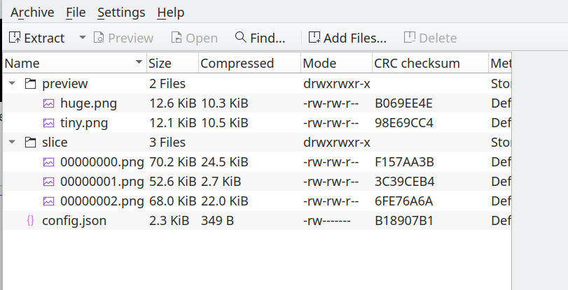
- Create a zip archive (example: pcb_prototype.zip) with config.json and the subdirectories preview and slice at the root. Figure 4 illustrates the zip archive structure.
- Rename pcb_prototype.zip to pcb_prototype.uvp: This is now a valid uvp file and the output of this step.
|
|
Figure 4: Structure of the zip archive that becomes the .uvp file, illustrated with Kubuntu's Ark archive management gui.
|
To save you some time, here are my huge.png 800x480 preview, the tiny.png 400x400 preview, and the all-important config.json control file. The config.json file must be edited to suit your printer and PCB material. Experimentation may be necessary.
7. Create the 3D printer file for printing
This step is short. You need to know the file format for your 3D printer -- in my case, cxdlp. Open the UVTools app. Use it to open the just-created fie "pcb_prototype.uvp". Use UVTools' Convert to -> cxdlp -> Creality cxdlp and choose version 3 (for my specific printer). Save as pcb_prototype.cxdlp and transfer the file to the 3D printer.
This step concludes the file preparation. Proceed to Part 3 of this article for the steps to expose the PCB, some notes and tips, and some photos of PCB manufacturing results.
Back to Part 1 of this article.
Copyright notice: All information, images, and downloadable files are licensed under the Creative Commons License CC-BY-SA.
 00000000.png
 00000001.png
 00000002.png