Continued from Part 2 -- Step-by-step creation of the 3D printer file.
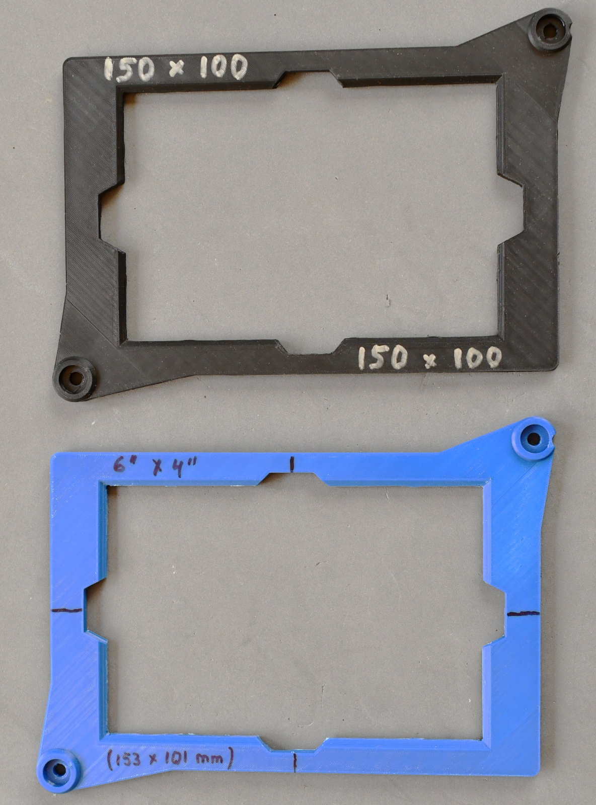
For a single-sided PCB, the PCB could be placed above the PCB pattern, but the matter gets slightly more complicated for double-sided PCBs since the two layers need to be aligned. I had best results with a frame that is attached in the place of the resin vat and that holds the PCB exactly centered. The downside is that each PCB size needs its own exposure frame, examples of which are shown in Figure 5.
|
|
| Figure 5: Frames to hold a PCB centered above the print screen. Mounting holes match those of the resin vat. Click on the image to access a full-size version. |
It should be possible to design a frame that can be adapted for any PCB size and aligned so that the PCB sides are aligned for exposure. Such a frame needs several adjustment points: two sides that adjust to the PCB size, and an overall translation/rotation adjustment for alignment with the screen. I believe that the overall effort is less to have one frame for each PCB size in use. Never the less, even in this case, some trial-and-error can be expected until the inner part of the frame aligns with the screen center.
|
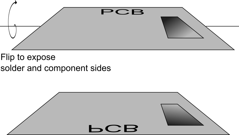
| Figure 6: Illustration of flipping the PCB between exposure of the solder side and the component side. |
Exposing a double-sided PCB takes the following steps:
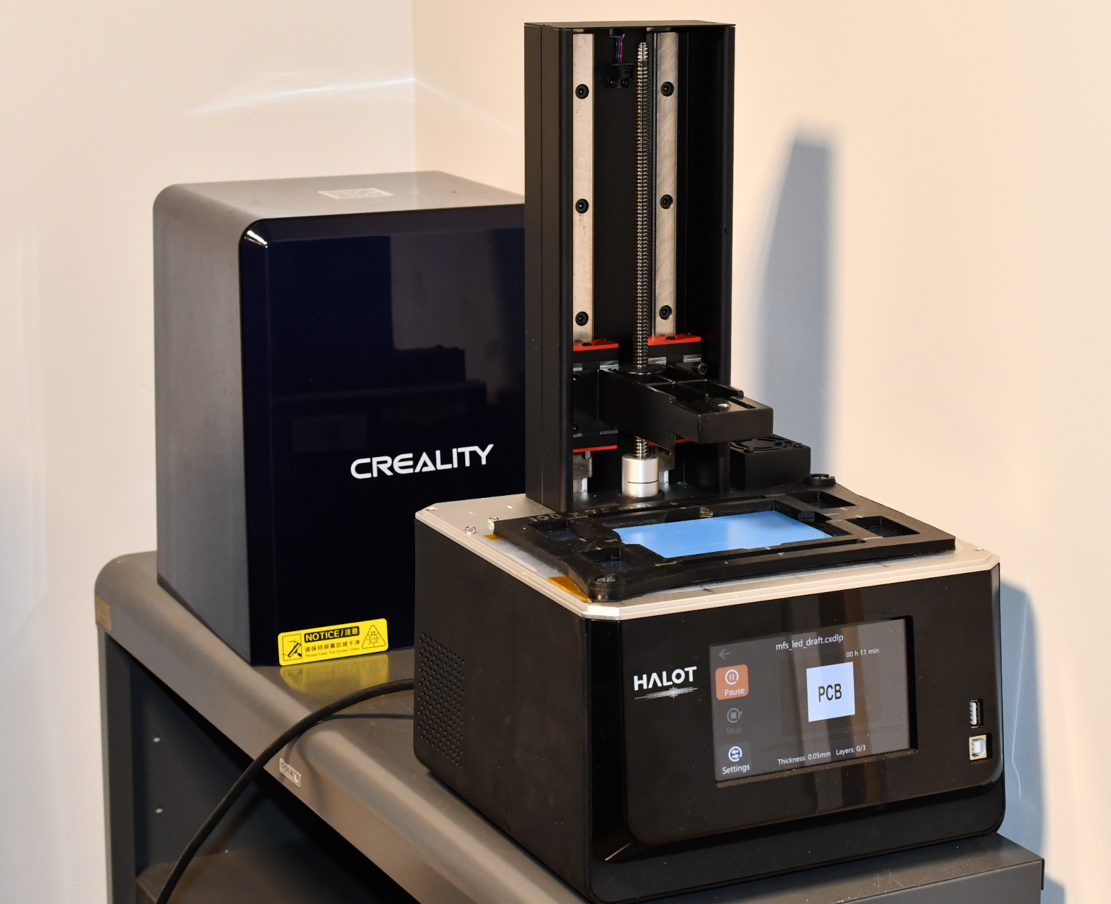
Figure 7 shows the Halot-One resin printer in its modified form -- resin vat and build plate removed, a PCB frame mounted in place of the resin vat with a piece of protective FEP foil underneath frame and PCB. The touchscreen display of the printer displays the "tiny.png" icon with the letters "PCB". The photosensitive PCB is in place with the solder side facing down (blue protective foil removed), and the component side is facing up, the protective foil still in place.
|
| Figure 7: The Halot-One Plus exposing a PCB. The touchscreen displays the "tiny.png" preview. The build plate has been removed, and the vat replaced by a PCB exposure frame. The PCB is visible inside the frame by the blue color of its protective foil. The PCB fits snugly, but not tightly, into the frame. Click on the image to access a full-size version. |
Once you immerse the PCB, you should see clouds or swirls of dissolved resin lift off of the PCB. Agitate the liquid gently to better wash off the photoresist. When the exposed pattern is clearly visible and the developer no longer creates any clouds, take out the PCB from the bath and rinse with plain water. Avoid scratching the photoresist!
If you experience unexposed regions of photoresist come off, the PCB may have been overexposed or the developer solution is too strong. Conversely, if not all photoresist is removed from the exposed regions, the PCB may be underexposed or the developer too diluted or too old.
Etching: Exposed copper needs to be removed by chemical etching. Ferric chloride is commonly used, but I have better experience with ammonium persulfate. It appears to have less over-etching at the edges (where the etchant goes underneath the photoresist), and it is generally less of a hellish mess than ferric chloride. Some custom DIY recipes exist, which may involve hydrochloric acid and hydrogen peroxide, but we are now looking at very corrosive and toxic chemicals, which should discourage use of those recipes.
The etching solution has an appreciably high concentration of 250 grams of ammonium persulfate in 1 liter of water (approximately 1:5 ratio!). The etching process should proceed rapidly to avoid over-etching and erosion of the photoresist. For successful etching, it is important to
A NOTE OF CAUTION: These chemicals are dangerous. They are highly corrosive. NaOH is caustic. Ammonium persulfate is an oxidizer. Personal protective equipment (lab safety glasses, protective latex or nitrile gloves) are absolutely required. Developing and etching should take place on a stable, chemically resistant surface that can be easily cleaned in case of an accidental spill. Chemicals must be stored in accordance with safety regulations (at the minimum, stored in glass containers, which are in turn placed in secondary containers. Use a separate secondary container for the etchant). Used solutions must be disposed of as hazardous waste according to applicable laws and regulations.
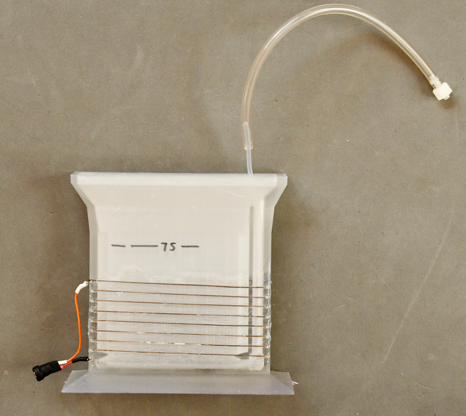
I found it useful to 3D-print cuvettes that fit the PCB size and thus allow etching with the least amount of etching solution. Figure 8 shows a cuvette for 100 x 75 mm PCBs. The cuvette can be filled with 100mL etching solution. Resistance wire repurposed from an old toaster is used for heating (a 19V laptop power supply provides sufficient voltage and has ample current capacity). A Teflon tube runs along the bottom, into which I pierced small holes at regular intervals. A small membrane pump can be attached to provide aeration.
|
| Figure 8: Etching cuvette for 100 by 75 mm PCBs. The cuvette is narrow and fills with less than 100mL etchant. Resistance wire scavenged from an old toaster is wrapped around the cuvette to allow heating. Teflon tubing leads inside the cuvette for aeration. Click on the image to access a full-size version. |
Drilling: A precision drill press with high-speed PCB drill bits is required. These drill bits are small: 0.6 mm for vias, IC sockets, and small through-hole components; 0.9 mm for larger components, pins, and headers. These drill bits break easily. The center hole of pins and vias should be small, because it serves only as a drill guide -- the final hole diameter is determined by the drill bit. Note that the method described in this article does not include plating of vias. Therefore, all vias must be connected with a small piece of wire. The drilling step is where layer alignment becomes crucial: If the layers are not aligned, the drill misses on one layer. Also, even for small drill sizes, a generous pad size is helpful. If space allows, I am using 80 mil (2mm) pad diameter even for 0.6mm drills. For IC sockets and headers, my preference are oval or elongated pads that provide sufficient support surface for the solder.
Yet on my to-do list: Would it not be possible to use a CNC router for drilling? The alignment problem would return, and drill bits would need to be exchanged manually. However, a drill file is produced by the PCB layout software that contains all drill coordinates, so it should be possible to write a script to read the drill coordinates and write, say, a grbl or gcode file... any takers?
|
|
| Figure 9: Boost converter that I used for the layout examples in Figures 1 through 3. Top: PCB after etching and with vias and through-holes drilled. Some components have been loosely placed, but not soldered. Bottom: Completely populated PCB with all vias wired through. Click on either image to access a full-size version. |
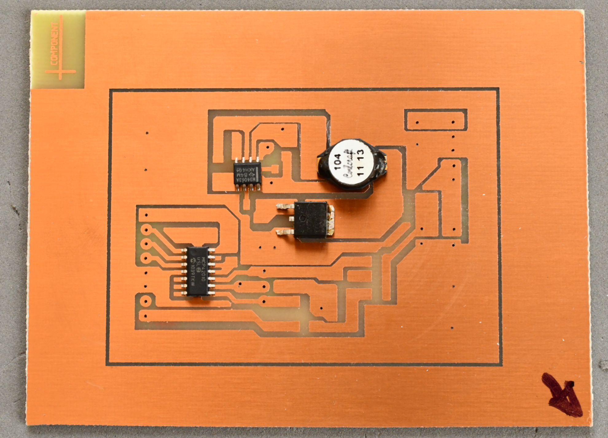
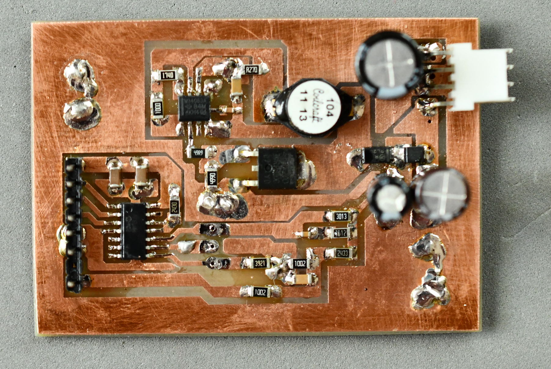
The example layout in Part 2 (Figures 1 -- 3) can be seen in Figure 9. Figure 9 (top) shows the PCB after etching and with vias and through-holes drilled. Some components have been loosely placed, but not soldered. The bottom right arrow was used to explore alignment issues, but none were found. Note how well-defined the letters in the top left corners have been etched. Figure 9 (bottom) shows the same PCB, cut to size and fully populated. As can be seen from the ICs, a 50-mil pin pitch is nowhere near the limits of this fabrication method.
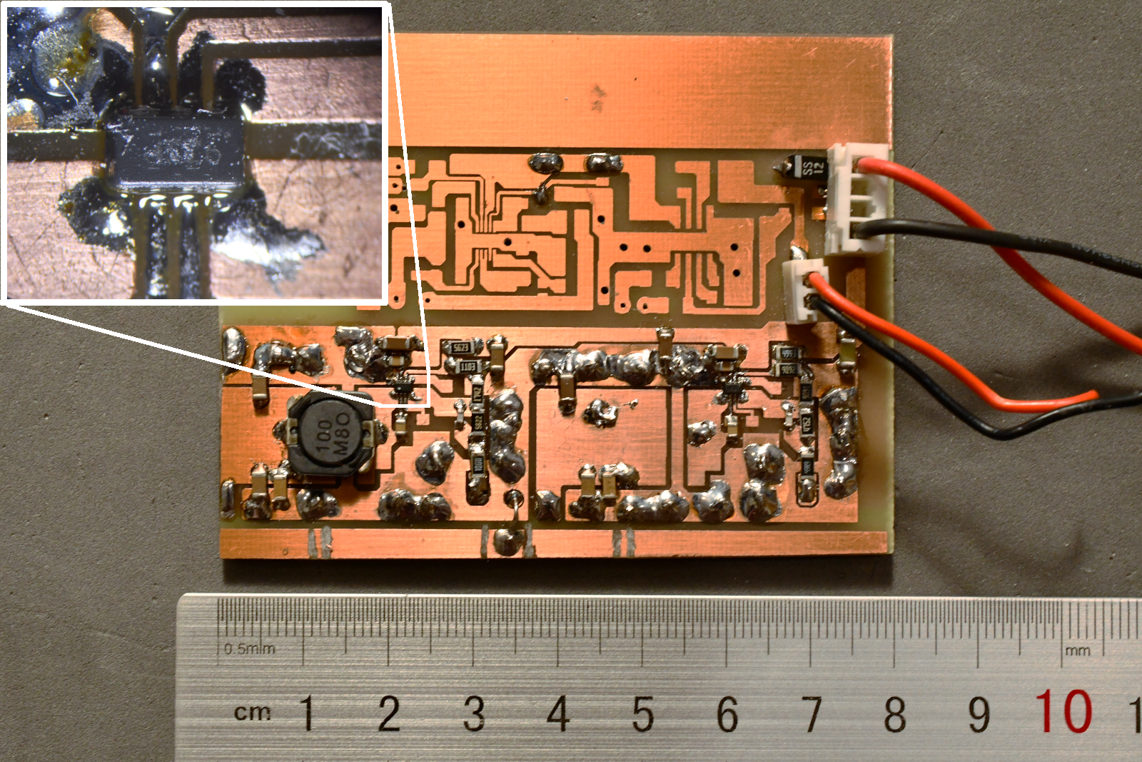
Figure 10 shows a different board; in this case, one IC is present in a SOT-5x3 package with pins less than 0.25 mm in each direction and 0.5 mm pin pitch. The IC is shown under the microscope in the inset. The IC itself is only 2 mm wide by 1.3 mm high. In the not-yet-populated area, a pattern is provided for a 10-pin DFN package (3 x 3 mm) that also has a 0.5 mm pin pitch and 0.25 mm wide pins. the VCC trace (top, pin 8) was not fully separated from the trace to pin 9, and some minor copper residue was removed with a scalpel.
|
| Figure 10: PCB for a group of DC-DC converters. The lower part is populated. One IC in a SOT-5x3 package is shown under microscope magnification (inset). In the not-yet-populated area, a pattern to accommodate a 10-pin DFN package with 0.5 mm pin pitch can be seen. Large through holes are 0.9 mm, and some are used to connect component-side ground to the solder-side ground plane with 0.9mm thick, thermally conductive wire. Click on the image to access a full-size version. |
Back to Part 2 or Part 1 of this article.
Copyright notice: All information, images, and downloadable files are licensed under the Creative Commons License CC-BY-SA.